
 NANOTECHNOLOGY
AND GRAPHENE
NANOTECHNOLOGY
AND GRAPHENE
The Japanese physicist Norio Taniguchi of Tokyo Science University, in 1974, was the first to introduce the term "nanotechnology", to describe the production of nanoscale materials, namely materials that have dimensions equal to one millionth of a millimeter (1 nm = 10-6 mm) and one billionth of a meter (1 nm = 10-9 m).
However, the concept of nanotechnology was born in December 1959, during a conference held by the physicist Richard Feynman at the California Institute of Technology (Caltech); in that occasion he predicted the ability to control the matter and to realize nanoscale devices. In his speech, entitled "There's Plenty of Room at the Bottom", Feynman talked about the "problem of manipulating and controlling the small-scale things"; he claimed that the physics principles were not in contradiction with the ability to manipulate and to build objects "atom by atom". In that occasion he pronounced the famous phrase: "What would happen if we could arrange the atoms one by one the way we want them? …".
In 1986, Kim Eric Drexler, in his book "Engines of Creation: The Coming Era of Nanotechnology" promoted the technological relevance of the nano-scale phenomena. His idea of nanotechnology is defined as "Molecular NanoTechnology” and refers to mechanical systems at the molecular scale, that are designed and built “atom by atom”. An application of Molecular NanoTechnology is "utility fog":
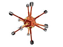 it
is a cluster of nano-robots that interact each other through a
software able to change their position inside the cluster, to which
they belong, so that it takes, on request, different shapes.
it
is a cluster of nano-robots that interact each other through a
software able to change their position inside the cluster, to which
they belong, so that it takes, on request, different shapes.
Nanotechnology is therefore a branch of the applied science and technology able to manipulate and organize the smallest elements of the matter. In practice, nanotechnology examines the methods and the techniques to control the matter in the atomic and molecular scale and it is able to create structures “atom by atom”, having a new organization. The dimensions of the nano-materials have a range between 1 to 100 nanometers.
The milestones in the nanotechnology field are summarized below:
1959 - Richard Feynman gives his speech "There's Plenty of Room at the Bottom".
1974 - Norio Taniguchi introduces the word "nanotechnology".
1981 - Gerd Binnig and Heinrich Rohrer realize the Scanning Tunneling Microscope - STM at the IBM Zurich Research Laboratories. This kind of microscope was the first instrument capable of displaying images of individual atoms. Binnig and Rohrer, for this discovery, received the Nobel Prize in Physics in 1986.
1985 - Richard Smalley, Harold Kroto and Robert Curl discover the fullerenes (Nobel Prize in 1996).
1986 - Gerd Binnig, Calvin Quate and Christoph Gerber invent the Atomic Force Microscope - AFM.
1990 - The first newspaper on nanotechnology is published.
1991 - Sumio Iijima discovers the carbon nanotubes.
1993 - The first Nanotechnology Laboratory is founded at the "Rice University” (USA).
2004 - A single layer of graphite is isolated and called graphene.
2010 - Anrej Gejm and Konstantin Novosëlov get the Nobel Prize for their studies on graphene.
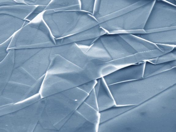 This
image
looks
like silk, stretched on the surface, but it represents a graphene
sheet on a silicon wafer
and
it has been obtained by a Scanning
Electron
Microscope
- SEM.
This
image
looks
like silk, stretched on the surface, but it represents a graphene
sheet on a silicon wafer
and
it has been obtained by a Scanning
Electron
Microscope
- SEM.
UNDERSTANDING “THE NANOSCALE”
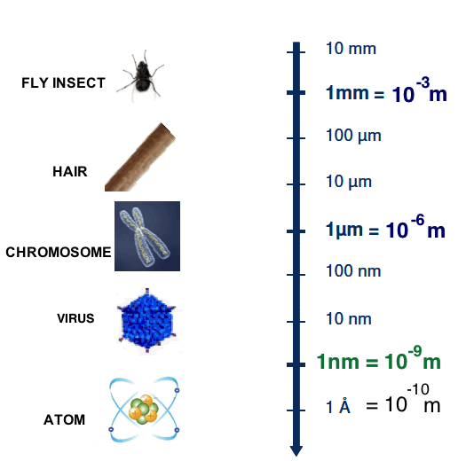
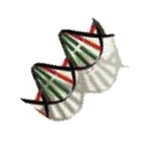
The reality in which we live involves sizes that, in principle, range from millimeter (mm) to kilometer (Km); these dimensions are far from one nanometer (nm), that is fifty thousand times smaller than the diameter of a hair. It is known that the eye of a needle has the dimensions of a million nanometers; a red blood cell is about one thousand nanometers; a DNA fragment is a few nanometers long and contains all the information necessary for the development of an entire living organism; finally, an atom has a size of about a tenth of a nanometer and a spherical object with a diameter of few nanometers is composed of a few thousand of atoms. Therefore, with nanotechnology we are in the world of the invisible to the human eye, practically in the context of structures composed of individual molecules or atoms; the advantage is that, in the nano-electronic devices, a smaller distance between interacting particles implies an increase of the operation speed and a less waste of energy.
GRAPHENE: “THE WONDER MATERIAL”
Watch the video: Introducing Graphene
Graphene is a single layer of carbon atoms, it is one atom thick (0,1 nm - 0,5 nm) and the carbon atoms, in the structure, are arranged in an hexagonal lattice. Graphene was produced in the laboratory, for the first time, starting from the graphite, that represents the most common form of carbon and that is the material of the pencils.

Graphene owns very high potentialities, for this reason its nickname is "wonder material". It is one of the lighter and thinner materials existing in nature, it is transparent, stronger than steel, very flexible, impermeable to liquids and gases and also excellent conductor of heat and electricity. The graphene potentialities are object of study in the Departments of Research and Development of many Companies and in many American and Asian Universities.
Find out more: What is graphene?
